
Cuk-Linear Dual Reactor
Technical reference: dual-rail power supply
Every audio board in the Malice Madrigal runs on ±15 V with a real ground. The Reactor makes those rails from an ordinary pedal supply and cleans them before they reach the music.
On this page
Evidence scope. The supply curves are analytical illustrations from the existing design reference. Connector impedance, ripple under load and whole-pedal noise are not specified here as measured results. See the measurement summary.
1. What the board does
The Ćuk-Linear Dual Reactor turns an ordinary 9 V pedal supply into the ±15 V rails every audio board in the pedal runs on. Each op amp gets +15 V and −15 V with the signal referenced to a real ground, which doubles the room every stage has to swing and lets the stages connect without coupling capacitors.
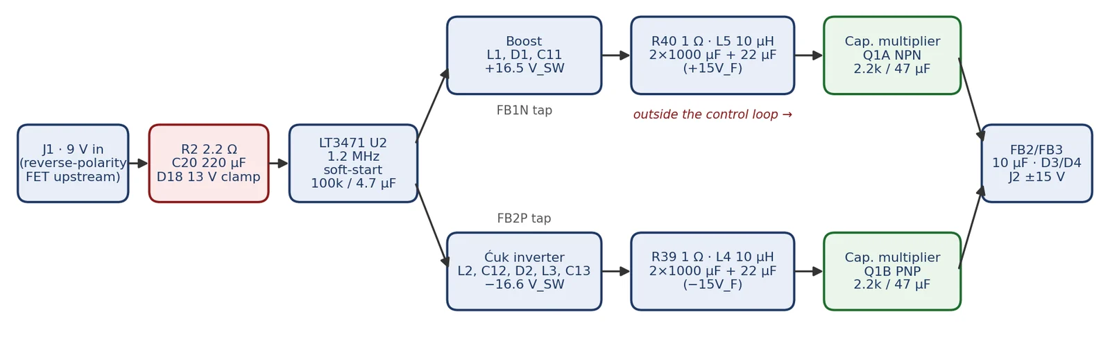
One LT3471 controller makes both rails: a boost converter for the positive rail and a Ćuk inverter for the negative rail. Each rail then passes through an R–L–C filter, a capacitance multiplier and a ferrite bead before it leaves the board. Regulation is sensed before the filters, so their large capacitance never touches the control loop.
1.1 Key figures
| Parameter | Value |
|---|---|
| Input | 9 V pedal supply, or a regulated 12 V supply |
| Outputs | ±15 V with a real ground |
| Load | about 28 mA per rail in normal use, 60 mA per rail maximum continuous |
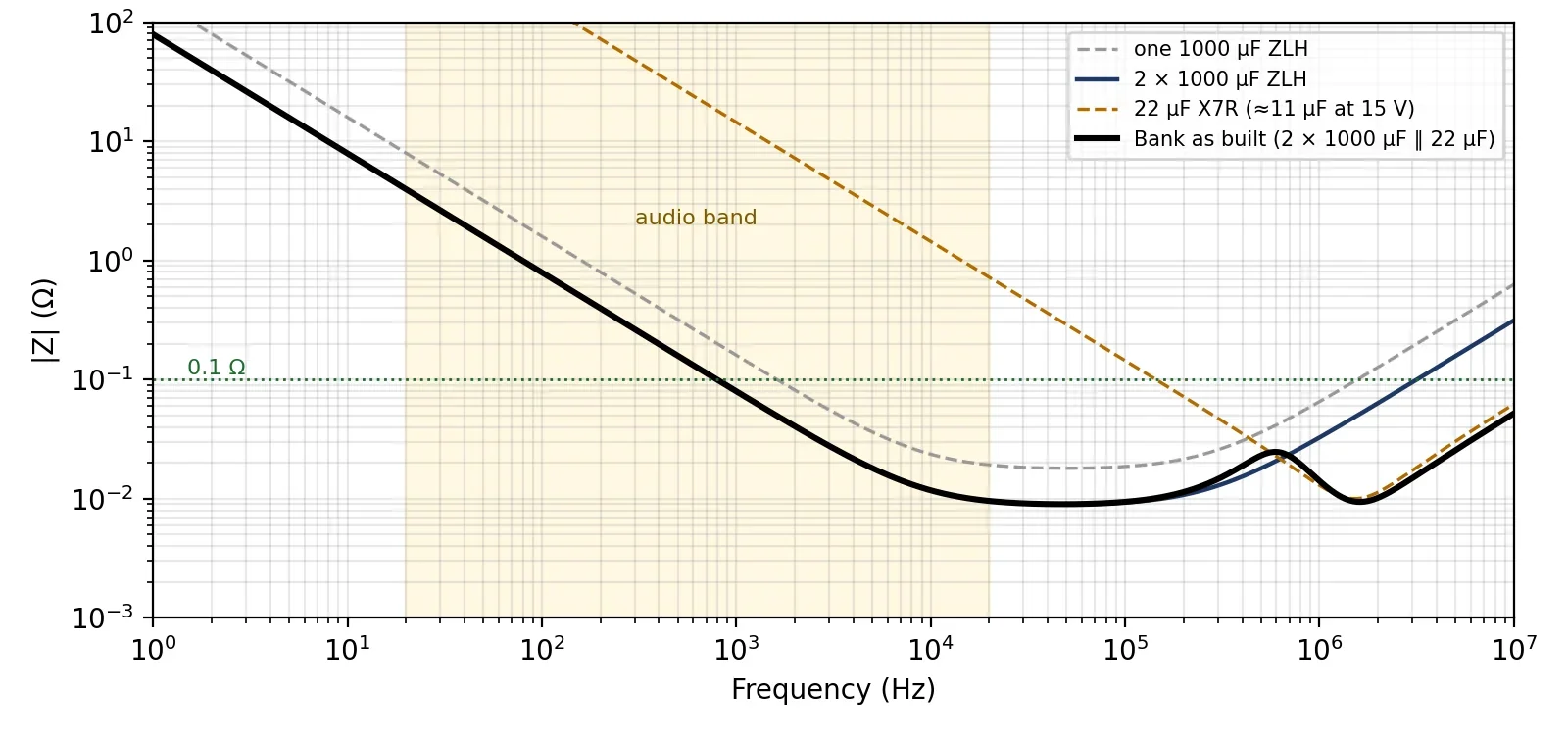
| Rail impedance | No measured connector-impedance specification. The bank plot describes a different node before the multiplier; the complete J2 impedance depends on frequency and load. |
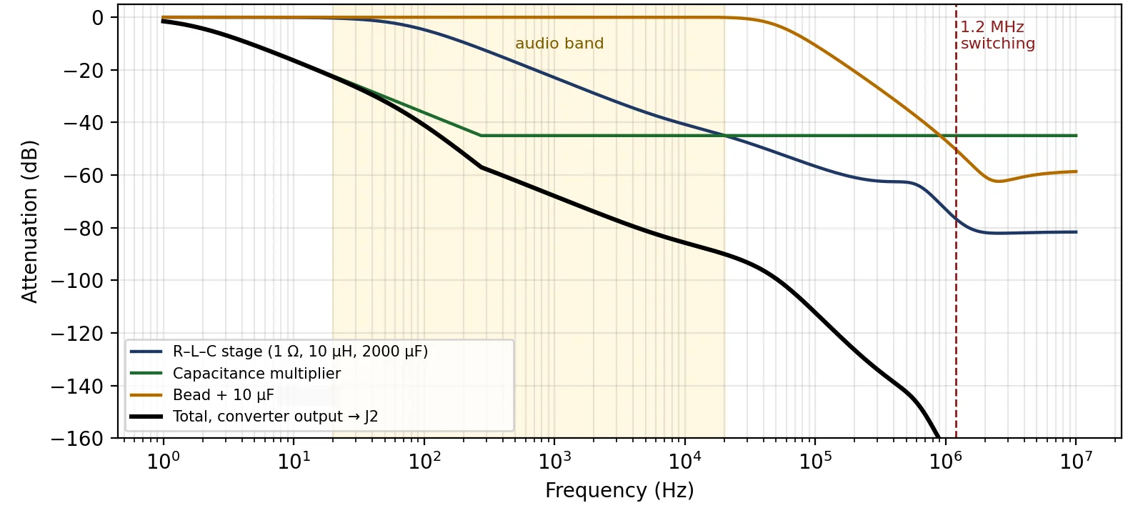
| Switching | LT3471 nominal switching frequency 1.2 MHz. Attenuation of the switching residue is illustrated by the circuit model; no measured ripple-under-load specification is supplied here. |
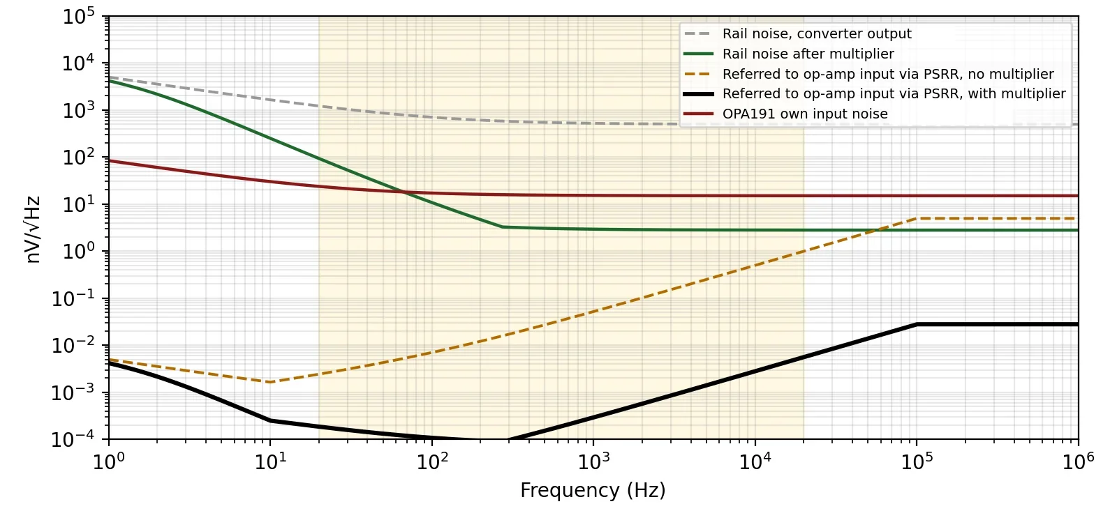
| Low-frequency rail noise | about 40 dB lower again after the capacitance multipliers — estimate from the circuit model, not a measured ripple specification |
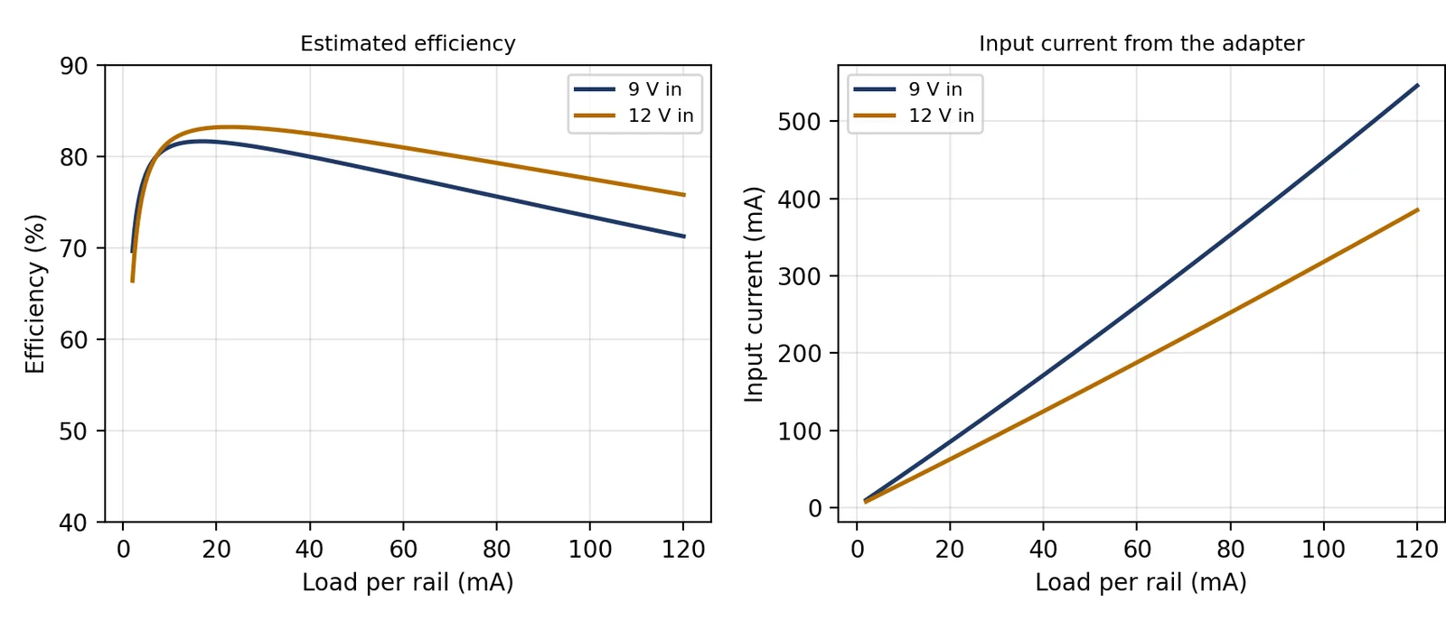
| Efficiency | about 80 % |
| Start-up | about 0.2 s to full rails, up to 0.4 s on a 300 mA adapter |
| Board | 60 × 23 mm, six layers, 48 parts |
2. How it works
2.1 Input
Power arrives from The Drive of Malice main board, which carries the DC jack and the reverse-polarity protection. On this board it passes through R2 (2.2 Ω) into C20 (220 µF), C2 (10 µF) and C6 (100 nF) at the LT3471. R2 and C20 form an input filter near 330 Hz and limit the inrush into the large capacitors when the pedal is plugged in. D18, a 13 V zener across the converter input, is an over-voltage clamp.
2.2 Controller and soft-start
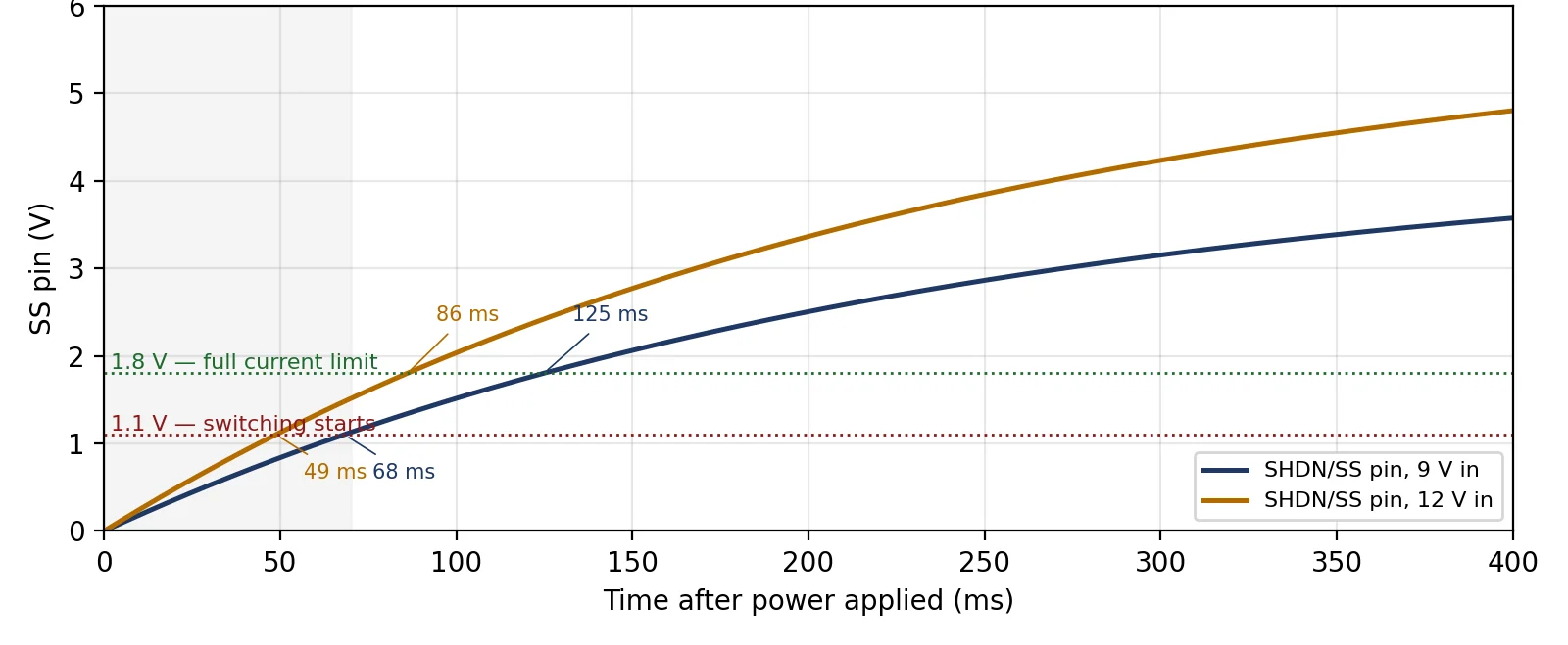
The LT3471 holds two 42 V, 1.3 A switches on a shared 1.2 MHz oscillator, with separate error amplifiers for the two rails. Each channel soft-starts through 100 kΩ and 4.7 µF: switching begins about 70 ms after power at 9 V, and the current limit is fully released by about 125 ms.
2.3 Positive rail
L1 (10 µH), D1 and C11 (22 µF) form a boost converter, regulated to about +16.5 V by R33 and R34 (232 kΩ and 15 kΩ): Vout = 1.00 V × (1 + R33/R34). The filter and multiplier after it bring the rail to +15 V at the connector.
2.4 Negative rail
L2, C12, D2, L3 and C13 form a Ćuk inverter, regulated to about −16.6 V by R35 and R36 (15 kΩ and 249 kΩ): Vout = −1.00 V × R36/R35. C12 carries the energy from input to output and sees about 26 V at 9 V in, hence its 50 V rating. Because the output current flows through L3, the raw ripple is about four times lower than the boost’s, and there is no DC path from input to output.
2.5 Output filter
Each rail passes through a 1 Ω / 10 µH filter and a bank of two 1000 µF capacitors with 22 µF ceramic. The existing transfer model predicts substantial rejection of the 1.2 MHz switching residue. The capacitor-bank impedance plotted below is frequency-dependent and refers to that node before the capacitance multiplier, not to the complete supply at J2.
2.6 Capacitance multiplier
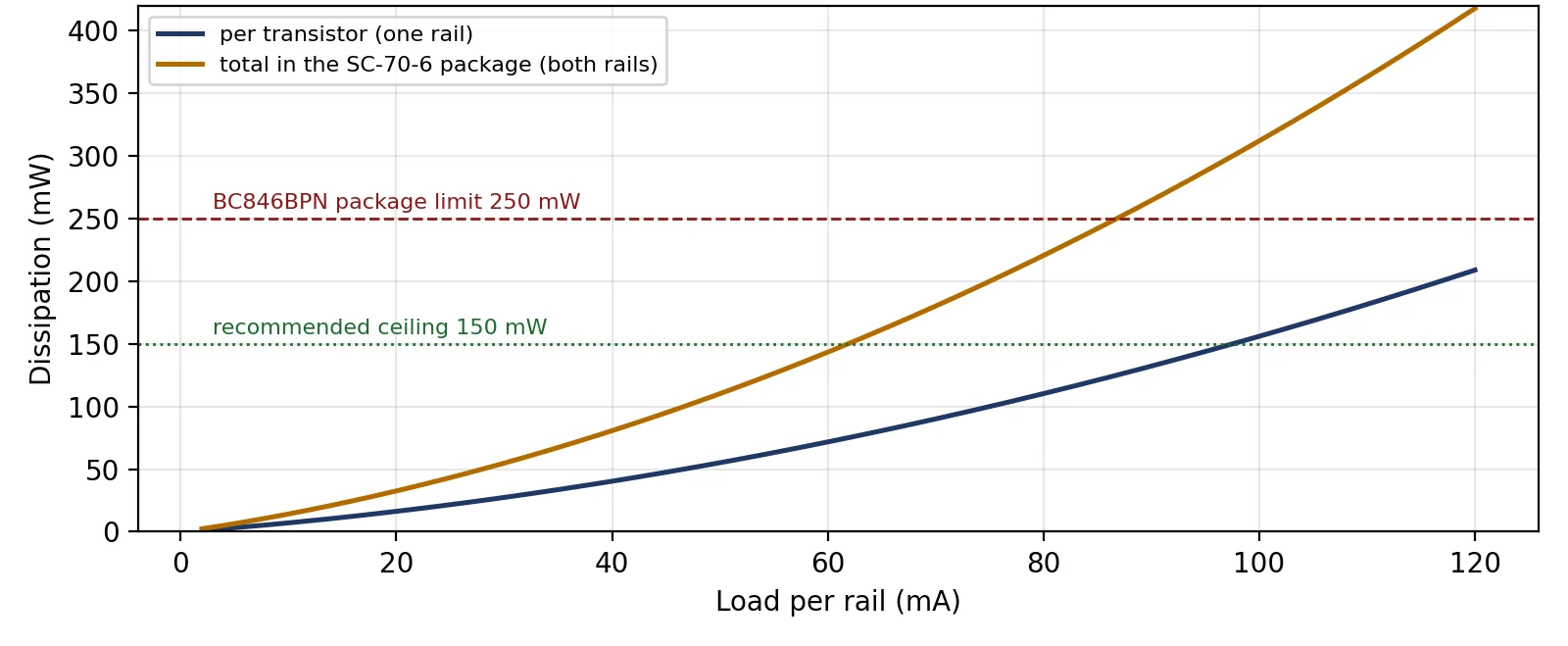
Q1, a BC846BPN with one NPN and one PNP, forms an emitter-follower capacitance multiplier on each rail. Its base is filtered by 2.2 kΩ and 47 µF. This is intended to reduce low-frequency ripple while the emitter supplies load current. It adds voltage drop and a frequency- and load-dependent output impedance; it is not an ideal regulator or capacitor.
2.7 What the audio boards see
The audio-board amplifiers provide additional power-supply rejection, which varies with frequency and device. The plot below combines a supply model with representative OPA191 rejection and input-noise data. It is an estimated noise budget; it does not establish measured rail ripple or assembled-pedal noise performance.
2.8 Output connector
Ferrite beads with 10 µF add a final high-frequency filter at the connector. D3 and D4 clamp reverse rail excursions if one rail collapses. They limit one fault mechanism, rather than guaranteeing that operation on a single rail is safe or damage-free.
3. Power and protection
Use a 9 V DC center-negative pedal supply, or a regulated 12 V supply, rated 300 mA or more; 500 mA gives extra start-up margin.
Pedal supplies come in 9, 12 and 18 V. This pedal is designed for 9 V or a regulated 12 V supply, so don’t plug in an 18 V supply. The input has limited over-voltage protection, but it isn’t guaranteed. Unregulated wall adapters can sit well above their label and aren’t supported.
A supply plugged in backwards is blocked on the main board before it reaches this board.
4. Ratings
| Parameter | Value |
|---|---|
| Input voltage | 9 V, or regulated 12 V (8.5 to 12.6 V) |
| Adapter rating | 300 mA minimum, 500 mA recommended |
| Output voltage | ±15 V |
| Output current, per rail | 28 mA typical, 60 mA maximum continuous |
| Rail impedance | No measured connector-impedance specification. The bank plot describes a different node before the multiplier; the complete J2 impedance depends on frequency and load. |
| Start-up to full rails | about 0.2 s; up to 0.4 s on a 300 mA adapter |
| Operating temperature | 0 to 50 °C ambient |
| Storage temperature | −20 to 70 °C |
The current rating is set by Q1: the SC-70 package’s recommended 150 mW ceiling is reached near 60 mA per rail.
5. Mechanical and connectors
| Item | Value |
|---|---|
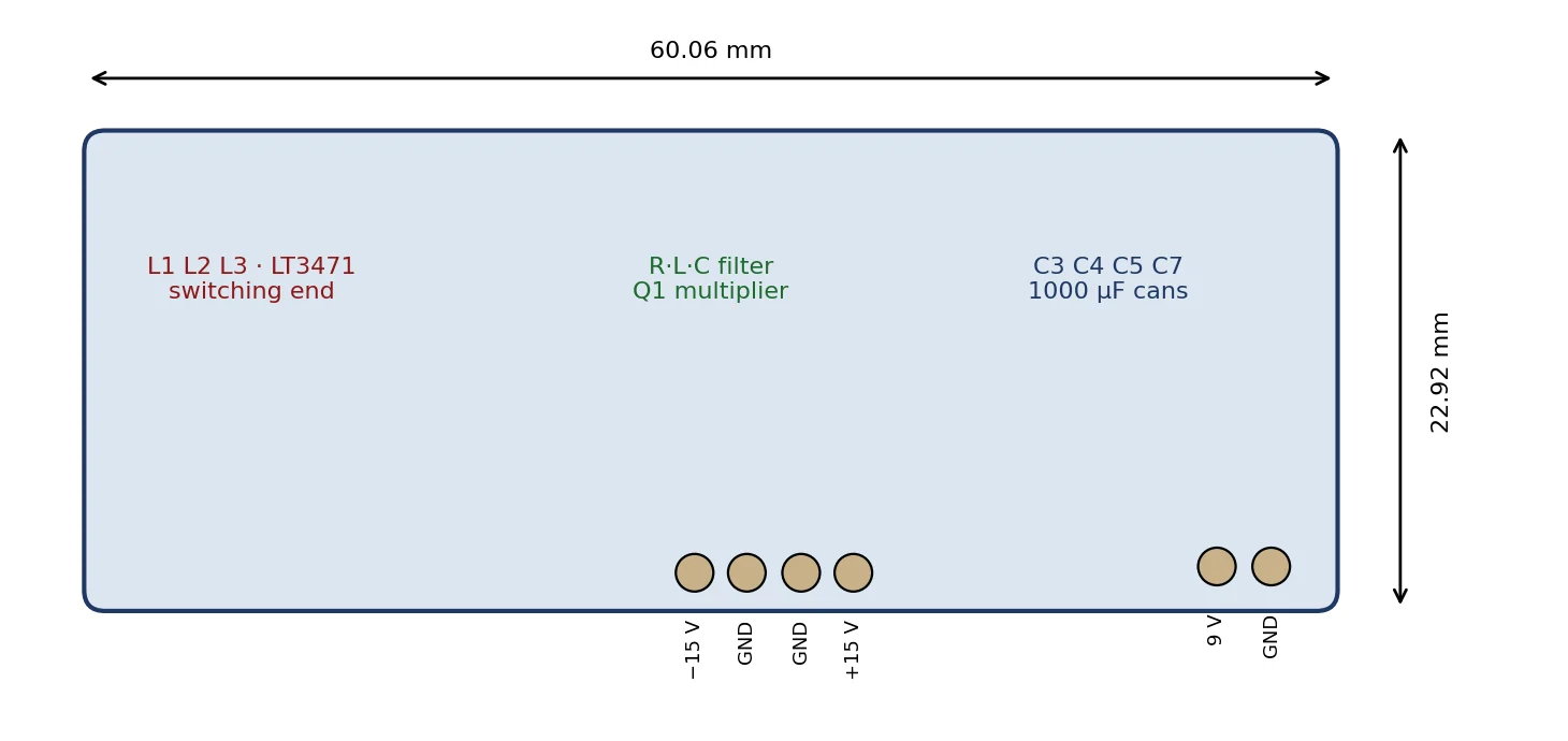
| Outline | 60 × 23 mm, six layers, 1.2 mm FR4; corners notched to clear the enclosure |
| Mounting | Stands on edge at the bottom of the enclosure beside Wall of Ice and Twin Assassins. The switching end (L1 to L3 and U2) faces away from the main board’s input-jack corner. |
| Tallest parts | the 1000 µF cans, 10 × 23 mm |
| J1, input | 1×2, 2.54 mm: pin 1 9 V (protected, from the main board), pin 2 GND |
| J2, output | 1×4, 2.54 mm: pin 1 +15 V, pins 2 and 3 GND, pin 4 −15 V |
| Weight | about 12 g |
6. Checking a board
With 9 V in and the audio boards connected, expect:
- about 8.7 V at C20;
- about +16.5 V at C11 and −16.6 V at C13, the converter outputs;
- ±15 V at J2;
- 1.00 V at VREF (pin 3), and about 4.3 V on both soft-start pins.
At power-up, switching starts after about 70 ms and both rails reach full value within about a quarter of a second. After ten minutes at normal load, U2 and Q1 are barely warm.
7. If something’s wrong
| Symptom | Check | Likely cause |
|---|---|---|
| No output, no input current | the voltage at C20 | R2 open after an over-voltage supply: check D18 for a short and replace both |
| +15 V at C11, missing or low at J2 | Q1 | Q1 damaged by a short on the +15 V rail: clear the short and replace Q1 |
| −15 V missing, +15 V fine | −15 V at C13; the SW2 waveform | D2 or C12: check D2’s orientation (anode to CUK_X) and C12’s 50 V rating |
| Both rails low, input current high | the voltage at C20 under load | adapter current-limited, or the input below 8 V |
| Rails stuck near +8 V and 0 V | the soft-start pins | the converter never started: soft-start pins below 1.8 V (R37/R38 open, C14/C15 shorted) |
| Whine or hiss on the audio boards | ripple at J2, probe tip and barrel on the pins | mounting coupling into the input jack, not the rails: reorient the board |
| Q1 hot | load current | load above 60 mA per rail |
| Start-up takes more than half a second | adapter rating | a 300 mA adapter: expected |
Before you plug in: power in the player’s guide and power and protection in the technical library